
 by
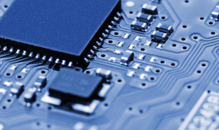
by The image sensor is one of the most important components in any digital camera. It captures the light coming through the lens and converts it into digital information that can then be processed by the camera. There are different types of image sensors but one of the most common is the shutter image sensor.
How Shutter Image Sensors Work
A shutter image sensor contains an array of light-sensitive pixels that are exposed to light entering through the camera lens. At the core of each pixel is a photodiode which accumulates and stores electric charge when exposed to light. The more light that hits a photodiode, the more electric charge it builds up.
In front of the photodiode array is an electronic shutter mechanism. The shutter opens and closes at timed intervals to control the duration of light exposure for the photodiodes. When the shutter opens, light is allowed to hit the photodiodes for a brief period known as the exposure time. Longer exposures allow more light and shorter exposures less.
After the exposure, the Shutter Image Sensor closes and the electric charge stored by each photodiode is sampled or read out by on-sensor electronics. The charge levels are converted to digital values that represent the brightness at each pixel location. This raw image data is then processed by the camera’s image processor for color processing, noise reduction, sharpening and so on before being saved as a photo file.
The electronic shutter then resets and the cycle repeats with the next exposure. This allows shutter image sensors to capture a rapid sequence of still photos at speeds up to thousands of frames per second for actions like slow-motion video.
Advantages of Shutter Image Sensors
Benefits of Shutter Image Sensors for Digital Photography
Some key advantages that shutter image sensors provide for digital photography include:
Exposure Control – The electronic shutter provides precise control over exposure times from fractions of a second down to microsecond levels. This allows capturing action shots with fast shutter speeds or long exposures for low light situations.
No Moving Parts – Since there are no physical moving parts like mechanical shutter curtains, shutter image sensors are more durable and reliable over the lifetime of the camera. They also have essentially no shutter lag between pressing the shutter button and image capture.
Global Shutter – All pixels are exposed simultaneously during the active period of the electronic shutter. This avoids the rolling shutter effect where parts of the image are exposed at slightly different times, preventing image distortion from fast motion.
High Speeds – Sampling charge from individual pixels allows extremely fast continuous shooting speeds up to thousands of frames per second for slow motion video. Mechanical shutters top out at less than 100 fps normally.
Simpler Design – Without mirrors or shutter curtains, shutter image sensors result in simpler optical systems inside cameras. This helps minimize size and maximize light efficiency through the lens.
Exposure Bracketing – By rapidly varying the exposure time across sequential frames, shutter image sensors enable HDR and exposure bracketing without needing multiple shots.
So in summary, shutter image sensors offer photographers unprecedented control over image exposures and capture capabilities far beyond what is possible with mechanical shutters alone. This has become a highly valued attribute in both consumer and professional digital cameras.
Evolution of Shutter Image Sensor Technologies
Advancements in Integrated Circuit Design
Early digital camera designs in the late 1990s and 2000s utilized CMOS (complementary metal-oxide-semiconductor) shutter image sensors due to their lower production costs compared to CCD (charge-coupled device) image sensors at the time. However, CMOS sensors had lower image quality with more noise and fixed pattern noise.
Advancements in integrated circuit design and production over the last two decades have significantly improved CMOS image sensor performance. Smaller feature sizes down to 10 nanometers and below have increased photodiode fill factors on pixel arrays for greater light sensitivity. On-chip ADCs (analog-to-digital converters) sample pixels in parallel for faster readout speeds.
Dedicated pixel-level analog signal processing now performs functions like noise cancellation and digital correction directly on the silicon. Backside illumination flips the sensor assembly to receive light through the unoccupied backside of the wafer for better light capture in smaller pixels.
These ongoing improvements have brought CMOS image sensors nearly on par or superior to CCDs in terms of image quality depending on the application. CMOS is also overall cheaper and more integrated in design, dominating the digital camera and smartphone camera markets today.
Future Advancements Targeting Higher Resolutions
Pushing Pixels Smaller
As smartphone and digital camera resolution requirements increase annually, future advancements aim to keep shrinking the physical size of pixels while maintaining high light sensitivity. Processing circuits are being placed between pixels to minimize lost active area.
Advanced semiconductor processes will soon reach 5nm and even 3nm resolution by the late 2020s. This allows doubling pixel counts within the same image sensor footprints used today. For example, a 100 megapixel full-frame sensor may fit within a surface area that previously only held 50 megapixels.
Finer pixel pitch also improves light capture for extended ISO ranges and low-light performance. Computational techniques like pixel binning can simulate even larger pixel effective sizes during processing. Future stacked sensor designs place processing circuits beneath the photodiode layer for maximum packing density.
Multi and ToF Sensors
Triple-layer stacks with individually filtered red/green/blue pixels promise over 200 megapixels with superior color fidelity in today’s standard sensor sizes. Time-of-flight (ToF) range imaging sensors complement traditional cameras by mapping depth within a scene.
ToF combines an infrared illumination matrix plus finely-tuned distance detection pixels for robust 3D scanning, spatial audio processing, and augmented reality applications. As costs lower, ToF is poised to become a mainstream addition across cameras, smartphones and other devices in the near future.
*Note:
1. Source: Coherent Market Insights, Public sources, Desk research
2. We have leveraged AI tools to mine information and compile it